Capabilities
Capabilities
Advanced Electron Microscopy
Laboratory
Sandia National Laboratories (SNL)Capability Expert
Josh SugarClass
CharacterizationNode Readiness Category
2: High-Temperature Electrolysis (HTE)2: Low-Temperature Electrolysis (LTE)
2: Photoelectrochemical (PEC)
1: Solar Thermochemical (STCH)
Description
The advanced electron microscopy capability at SNL utilizes electron-based methods to characterize the morphology, composition, and structure of materials. A variety of techniques are available including imaging, diffraction, energy dispersive spectroscopy, electron energy loss spectroscopy, electron tomography, in situ heating/biasing, electron back-scattered diffraction, and transmission Kikuchi diffraction, that enable investigation of materials at length scales that range from the sub nanometer regime (0.7 Å) to the millimeter-scale regime. In addition, our facilities enable characterization in all 3 spatial dimensions, in particular with the use of electron tomography and serial FIB sectioning. These techniques can provide simultaneous information about composition, electronic structure/valence, and structure in a single experiment.
Capability Bounds
Features smaller than 0.65Å are outside the spatial resolution of the best TEM available at Sandia. Samples larger than 6" x 6" x 1 cm are difficult to accommodate in any SEM available. Also, limitations exist for the size of a volume or area to be investigated and the pixel size. For example, to interrogate a material with a 1 nm spatial resolution would limit the total size of the area investigated to something less than a 1 square micron. However, if a material is investigated with a 2 µm pixel size, it is possible to look at larger total areas (~ 50 mm2). Also, the volumes that can be measured in a 3D experiment are limited to relatively small volumes (200 nm x 200 nm x 200 nm in a TEM and approximately 50 µm x 50 µm x 300 µm in an FIB/SEM). Samples that are extremely electron beam sensitive will have limited applicability of these techniques, however we do have capabilities for acquiring data with low dose that can be considered. In addition, for analysis at the highest spatial resolutions (<1Å), careful sample preparation is required to make electron transparent samples, and the compatibility of the sample material and the sample preparation technique need to be considered to obtain the highest quality data.
Unique Aspects
Our electron microscopy capability has many tools, but there are 3 that have unique aspects and provide flexibility for a range of sample types. Our dualbeam FIB/SEM has a high-resolution, monochromated SEM column with the ability to achieve 0.7 nm spatial resolution at 1 kV. The Ga ion column has a resolution of 2.5 nm at 30 kV. The system has an EDS/EBSD system that enables chemical and crystallographic site specificity when choosing locations for sample preparation or analysis. In addition, the system has 3 GIS sources, the typical C and Pt, but also Pd, which is a unique source selected for making electrical contacts to carbon-based nanostructures. Our low-pressure analytical SEM has an electrostatic lens design with an optionally activated immersion mode, which enables high-resolution of a wide range of sample types including magnetic samples and non-conductive samples. In addition to EDS and EBSD analytical capabilities, this SEM also has the ability to perform electron-beam lithography. Transmission Kikuchi diffraction (TKD) is also possible with the EBSD detectors on both SEM systems, which enables crystallographic mapping of samples with spatial resolution <10 nm. We have a wavelength dispersive spectroscopy (WDS) detector, which enables accurate standards-based compositional measurements on appropriately prepared samples. We also have a variety of in situ stages for the SEM that enable mechanical testing, vacuum transfer (samples can be kept in inert environments from FIB through TEM if needed), and in situ heating.
Our TEM is a monochromated, aberration-corrected 300 kV system with EDS and EELS, that is also operational at 200 kV, 120 kV, and 60 kV. The probe-corrector provides a spatial resolution of 0.65 Å at 300 kV in STEM. The monochromator makes an energy resolution for EELS of approximately 0.14 eV achievable (FWHM of zero-loss peak). The EDS system has 4 detectors with a collection solid angle of 0.7 sr, which enables compositional mapping with near atomic resolution. The EELS system has two detectors, a conventional CCD, capable of acquiring spectra at 1000 spectra/sec, and a CMOS detector for low noise, high-sensitivity measurements. The CMOS detector can also be used for imaging of beam-sensitive materials. The system has a variety of holders with special capabilities including a vacuum/inert gas transfer, in situ heating, and in situ biasing.
Availability
The electron microscopy capabilities at SNL CA are a shared resource used for a variety of work including our mission critical work. As such, all tools are typically fully utilized (≥40 hours/week). While priority must be given to our NNSA mission critical work, sufficient time is available for using these tools for basic science and work for other customers. With appropriate engagement of SNL staff members on a project, sufficient tool time can be easily scheduled as long as it is recognized that these tools are a shared resource.
Benefit
Briefly, electron microscopy is a tried and true way to characterize materials and it can be used to understand transport phenomena. These types of tools will be needed to understand the structure, composition, and morphology of water splitting materials.
Images

Figure 1. DualBeam FIB/SEM
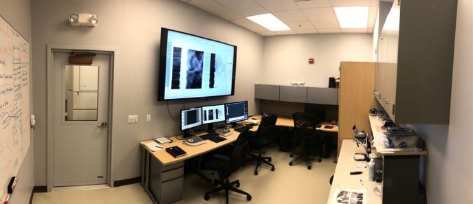
Figure 2. Titan Themis Z Control Room

Figure 3. Themis Z Microscope

Figure 4. Apreo Low Pressure SEM
References
1. Trindell, Jamie A., Mcdaniel, Anthony H., Ogitsu, Tadashi, Ambrosini, Andrea, and Sugar, Joshua D. Probing Electronic and Structural Transformations during Thermal Reduction of the Promising Water Splitting Perovskite BaCe0.25Mn0.75O3, accepted for publication in Chemistry of Materials, (2022) https://doi.org/10.1021/acs.chemmater.2c00731
2. Strange, N.A., Park, J.E., Goyal, A., Bell, R.T., Trindell, J.A., Sugar, J.D., Stone, K.H., Coker, E.N., Lany, S., Shulda, S. & Ginley, D.S. (2022). Formation of 6H-Ba3Ce0.75Mn2.25O9 during Thermochemical Reduction of 12R-Ba4CeMn3O12: Identification of a Polytype in the Ba(Ce,Mn)O3 Family. Inorganic Chemistry 61(16), 6128-6137.
3. Li, M., Hua, B., Wang, L.-C., Sugar, J.D., Wu, W., Ding, Y., Li, J. & Ding, D. (2021). Switching of metal–oxygen hybridization for selective CO2 electrohydrogenation under mild temperature and pressure. Nature Catalysis 4(4), 274-283.